PSRAM/ONFI/SDIO/EMMC/RPC

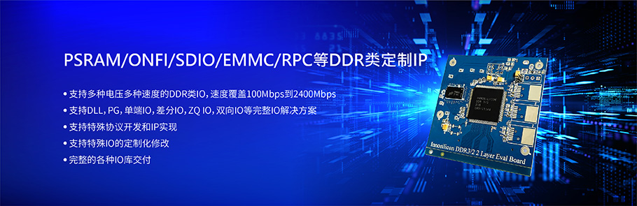
芯動(dòng)PSRAM/ONFI/SDIO/EMMC/RPC IP可(kě)提供支持JEDEC标準、兼容PSRAM器(qì)件的一站(zhàn)式交鑰匙解決方案,低功耗、高速率、小尺寸、時序優化。支持市場上所有的 APmemory UHS PSRAM組件。PHY組件包含PSRAM專用功能和(hé)實用 IO設備、關(guān)鍵時序同步模塊(TSM)、低抖動(dòng)PLL、PSRAM接口的TX和(hé)RX邏輯控制。且PHY都預先組裝了.lib、LEF和(hé)GDS,DQ總線帶寬可(kě)支持8位以匹配PSRAM DQ接口,易于集成,縮短(duǎn)客戶設計周期。該方案包括Controller和(hé)PHY,可(kě)配置時序、驅動(dòng)強度參數和(hé)各種PSRAM接口,靈活高效。

The INNOSILICON DDR IPTM Mixed-Signal PSRAM  PHY provides turnkey physical interface solutions for ICs requiring access to  JEDEC compatible PSRAM devices. It is optimized for low power and high speed  applications with robust timing and small silicon area. It supports APmemory  UHS PSRAM components in the market. The PHY components contain PSRAM  specialized functional and utility IO devices, critical timing synchronization  module (TSM), the low-jitter PLL, the TX and RX logic control for the PSRAM  interface.

Note that all INNOSILICON PHY is  pre-assembled with.lib, LEF and GDS so that it is very easy to integrate the  PHY with any existing SoC floor plan. The DQ bus width can support 8 bit to  match the PSRAM DQ interfaces. INNOSILICON is happy to pre-assemble each PHY  for our customer so that integration becomes extremely easy.

The Innosilicon's PSRAM PHY solution  includes PSRAM controller and PHY. With configurable timing and driving  strength parameters to interface to the wide variety of PSRAMs, the PHY is very  flexible with advanced command capability to increase PSRAM operation  efficiency.

KEY FEATURES:

  • PSRAM modes & signaling, rates from 200Mbps up to 1600Mbps

  • x8 data path interface

  • Multiple drive strengths adjustable

  • Supports read and write timing adjustments with soft calibration

  • Low latency with programmable timings for secure data handling

  • Per bit deskew support

  • Supports point to point memory sub systems and multi-rank

  • Support ZQ calibration to calibrate driver output resistance and  on-die termination resistance

  • PVT compensation and timing calibration for all corner reliability

  • At speed BIST, scan insertion

  • Various power-down modes for low power including self-refresh  support

  • Low jitter with superior noise rejection

  • APB Port register access interface

  • Dual Row IO implementation and more

  • Supports both wire-bond and flip- chip packaging

  • Wire-bond speed is package limited

  • Fully pre-assemble design, Drop-in hard macro to ease integration  and speed time to market

  • Zero risk with robust ESD architecture

  • Maintains self-refresh I/O drive state during VDD power down

  • Extensive EDA tool support for various design automation flows

  • Optional /CE retention mode permits VDD and all non-essential I/Os  to be powered down while retaining the external PSRAMs in self refresh mode

  • DFI compliant memory controller interface

  • Flexible pad ring configuration to adapt for various design and chip  scenarios

  • Integration with other INNOSILICON interface IP

  • Takes full advantage of process power savings and speed capability

  • Best in class low noise design to ensure best timing margin and  signal integrity

  • DFT functions to reduce test time and ensure high test coverage

  • Several programmable PHY operating modes through simple register  interface

  • Per Bit De-skew to improve composite data eye during read cycles at  high speed

INNOSILICON ADVANTAGES:

  • Fully customized solutions including Controller and PHY

  • Over 500,000 wafers shipped out with Innosilicon PSRAM IP

  • All major processes fully covered, such as 110nm, 55nm to 28nm,  22nm, 14nm, 12nm, 8nm, 7nm, 6nm, 5nm.

  • Full harden PHY proven by 100+ tapeouts

  • Simple integration with pre-assembled PHY

  • Low IO pin count

  • High performance

  • Test chip and FPGA integration services available

EXAMPLE APPLICATIONS:

一鍵啟動(dòng),簡化您的下(xià)一個(gè)産品設計流程!


聯系
我們

定制
需求