Chiplet (INNOLINK™)

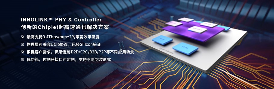
Innosilicon INNOLINK™ IP 提供領先的小芯片Chiplet IP解決方案,允許大量低延遲數據在較小的芯片之間無縫傳輸,就好像它們都在同一條總線上一樣。小芯片被定義為構成大型芯片的獨立功能塊,在這個(gè)異構集成新時代實現性能和(hé)效率提升的關(guān)鍵。基于此,Innosilicon 推出了 INNOLINK™ Chiplet解決方案,為數據中(zhōng)心、網絡、5G、HPC 和(hé) AI 應用程序提供裸片到裸片  (D2D)、芯片到芯片 (C2C)、闆到闆 (B2B)、以及封裝到封裝(P2P)高效能的連接。

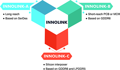
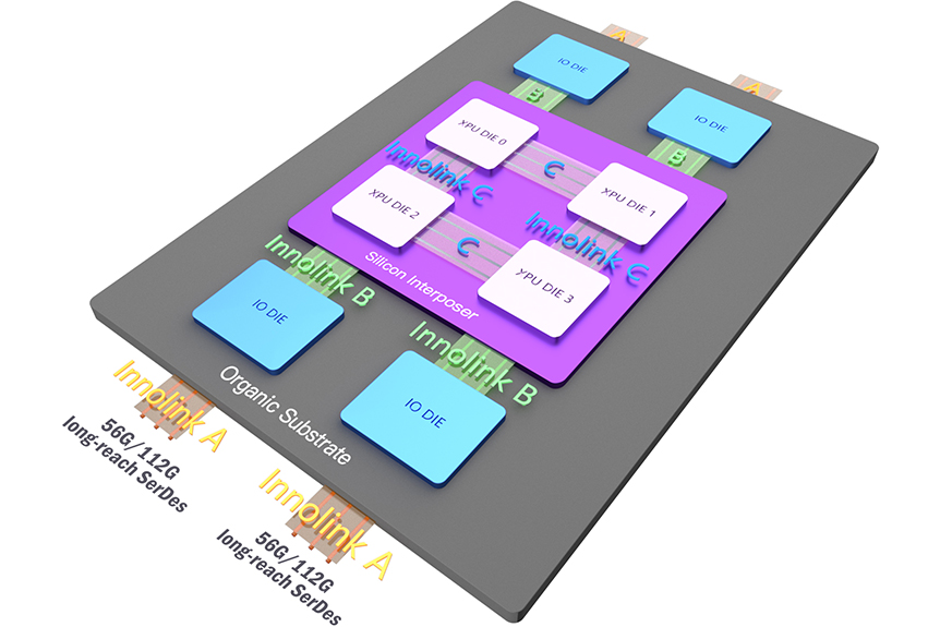
與當今可(kě)用的其他接口相比,Innosilicon INNOLINK™ IP 旨在以更低的功率和(hé)更小的面積預算最大限度地提高裸片/芯片/闆/封裝之間的帶寬。通(tōng)過提供三種互連選項 (A/B/C),INNOLINK™  IP 可(kě)以通(tōng)過易于使用的系統界面根據客戶的不同要求進行定制。它的架構具有高度可(kě)編程性和(hé)靈活性,最高可(kě)實現高達 3.4Tbps/mm2  帶寬效率密度,同時保持信号完整性和(hé)低延遲。在您的系統中(zhōng)采用 INNOLINK™ IP 肯定會使高性能計算 ASIC/FPGA 受益,例如(rú) CPU、GPU、AI 加速器(qì)等等。

Innosilicon INNOLINK™ IP provides a leading-edge chiplet solution allowing massive  amounts of low-latency data to pass seamlessly between smaller chips as if they  were all on the same bus. Chiplets, defined as independent functional blocks  making up a large chip, are pivotal in this new era of heterogeneous  integration to achieve performance and efficiency gains. Based on this,  Innosilicon launches the INNOLINK™ chiplet solution as  a critical enabler of the power- and cost-efficient die-to-die (D2D),  chip-to-chip (C2C), board-to-board (B2B) and package-to-package (P2P)  connectivity for data center, networking, 5G, HPC and AI applications.

Innosilicon INNOLINK™ IP is designed to maximize bandwidth between dies / chips / boards  / packages, compared to other interfaces available today, at lower power and  smaller area budgets. By offering three interconnect options (A/B/C), INNOLINK™ IP can be tailored to customer’s different  requirements with an easy-to-use system interface. It is architected for high  programmability and flexibility, Maximum bandwidth efficiency up to 3.4Tbps/mm2 while maintaining signal integrity and low latency. Adopting  the INNOLINK™ IP in your system will definitely benefit  high performance computing ASICs/FPGAs, such as CPU, GPU, AI accelerator, and  much more.

INNOLINK SOLUTIONS:

KEY FEATURES:

    Innolink-B

  • Meets the performance, efficiency and reliability  requirements of C2C/P2P interconnects

  • Already silicon proven

  • Delivers up to 24Gbps/pin

  • Single-ended DDR

  • Burst data

  • Forward clock

  • Low latency, Low power mode

  • Supports both Flip-chip and Silicon interposer

  • Software-defined IO direction and signal swap

  • Supports C4 Bump pitch of 100um~180um

  • Power efficiency of 0.7~1.1pJ/bit

  • Area efficiency of 0.4~1.0Tbps/mm2

    Innolink-A

  • Meets the performance, efficiency and reliability  requirements of B2B/C2C interconnects

  • Already silicon proven

  • Delivers 56Gbps/pair with -36dB insertion loss

  • Leverages high-speed long reach SerDes

  • Differential signal

  • CDR based Rx

  • Optimized latency

  • Scalable to 4/8/16/32/64/128 lanes

  • PHY-independent training

  • Low power mode

  • Power efficiency of 1.8pJ/bit

  • Area efficiency 0.4Tbps/mm2

    Innolink-C

  • Meets the performance, efficiency and reliability  requirements of D2D interconnects

  • Already silicon proven

  • Delivers 24Gbps/pin, per bit training

  • Single-ended DDR

  • Burst data, Low latency

  • App D2D, 2.5D/3D chiplet

  • Optimized for silicon interposer

  • Ultra low power, no CDR, no data package head

  • 0.4V IO voltage

  • Software-defined IO direction and signal swap

  • Supports bits redundant and lane repair

  • Micro Bump pitch of 40um~80um

  • Power efficiency of 0.45pJ/bit

  • Area efficiency up to 3.4Tbps/mm2

INNOSILICON ADVANTAGES:

  • Available in any 40nm or below technology nodes

  • Significantly lower cost, shorter time to market, lower supply risks for OEMs and simpler architectural partitioning than the monolithic silicon integration

  • Offers leading performance, power, and area per terabit

  • Flexible configuration with support for silicon interposer, package substrate and PCB options

  • Customizable synthesis for any FPGAs and ASICs

  • Full support from IP delivery to production

EXAMPLE APPLICATIONS:

  • High performance computing (HPC) applications

  • Next-generation data center

  • Networking

  • 5G communication

  • Artificial intelligence / machine learning (AI/ML) applications

INNOLINK APPLICATION:

一鍵啟動(dòng),簡化您的下(xià)一個(gè)産品設計流程!


聯系
我們

定制
需求