LPDDR5/5X/4/4X

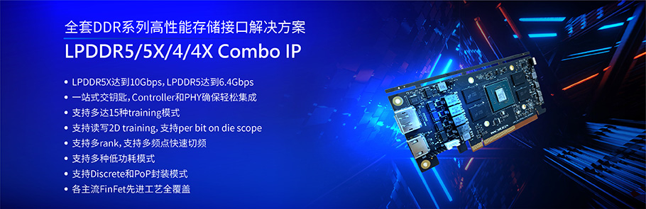
芯動(dòng)LPDDR5/5X/4/4X Combo IP可(kě)提供支持JEDEC标準、兼容SDRAM設備的一站(zhàn)式交鑰匙解決方案,低功耗、高速率、小尺寸、時序優化。支持市場上所有的 JEDEC LPDDR5/4 SDRAM 組件。PHY組件包含DDR專用功能和(hé)實用高性能I/O、關(guān)鍵時序同步模塊 (TSM) 和(hé)低功耗/抖動(dòng)DLL,可(kě)對任何SDRAM接口進行可(kě)編程細粒度控制。且PHY 都預先組裝了.lib、LEF和(hé)GDS,DDRn總線寬度可(kě)以從4位到80位或更多,易于集成,縮短(duǎn)客戶設計周期。該方案包括Controller和(hé)PHY,支持LPDDR5/5X/4/4X,可(kě)配置時序、驅動(dòng)強度參數和(hé)各種SDRAM接口,靈活高效。

The INNOSILICON DDR IPTM Mixed-Signal  LPDDR5/5X/4/4X Combo PHYs provide turnkey physical interface solutions for ICs  requiring access to JEDEC compatible SDRAM devices. It is optimized for low  power and high speed applications with robust timing and small silicon area. It  supports all JEDEC LPDDR5/4 SDRAM components in the market. The PHY components  contain DDR specialized functional and utility high performance I/Os, critical  timing synchronization module (TSM) and a low power/jitter DLLs with  programmable fine-grain control for any SDRAM interface.

Note that all INNOSILICON PHY is  pre-assembled with.lib, LEF and GDS so that it is very easy to integrate the  PHY with any existing SoC floor plan. DDRn bus width can be from 4 bit to 80  bit or more. INNOSILICON is happy to pre-assemble each PHY for our customer so  that integration becomes extremely easy.

The combo PHY solution includes DDRn controller and PHY, supporting  LPDDR5/5X/4/4X. With configurable timing and driving strength parameters to  interface to the wide variety of SDRAMs, the PHY is very flexible with advanced  command capability to increase SDRAM operation efficiency.

KEY FEATURES:

  • Max data rate: 10Gbps (LPDDR5X),  6400Mbps (LPDDR5) and 4266Mbps (LPDDR4/4X)

  • x16/x32/x64 data path interface extendable

  • 1.05V/1.1V JEDEC IO standard, support 1.05V and 1.1V LVSTL I/Os

  • support LPDDR4X 0.6V IO voltage and LPDDR5 0.5V/0.3V IO voltage

  • Support LPDDR5 WCK mode, Data copy, Write X and Link ECC features

  • Optional limited swing to VDDQ/3 in LPDDR4 mode

  • Independent read and write timing adjustments with auto calibration

  • Programmable write post-amble (0.5 tCK or 1.5 tCK)

  • Support both PoP and discrete memory package

  • Support various low power mode, support DFS and retention mode

  • Support point to point memory sub systems and multi-rank

  • PVT compensation and timing calibration for all corner reliability

  • At speed BIST, scan insertion, PAD and internal loopback modes

  • Various power-down modes for low power including self-refresh  support

  • Low jitter with superior noise rejection

  • APB Port register access interface

  • Support both wire-bond and flip- chip packaging

  • Wire-bond speed is package limited

  • Support different DDRn type signal mapping for feasible PCB layout

  • Fully pre-assemble design, Drop-in hard macro to ease integration  and speed time to market

  • Zero risk with robust ESD architecture

  • Maintains self-refresh I/O drive state during VDD power down

  • Extensive EDA tool support for various design automation flows

  • DFI4.0/4.1 compliant memory controller interface

  • Takes full advantage of process power savings and speed capability

  • Best in class low noise design to ensure best timing margin and  signal integrity

  • DFT functions to reduce test time and ensure high test coverage

  • Several programmable PHY operating modes through simple register  interface

  • Per Bit De-skew to improve composite data eye during read cycles at  high speed

INNOSILICON ADVANTAGES:

  • Fully customized solutions including Controller and PHY

  • Over 500,000 wafers shipped out with Innosilicon DDRn IP

  • All major processes fully covered, such as  28nm, 22nm, 14nm, 12nm, 8nm, 7nm, 6nm, 5nm.

  • Full harden PHY proven by 100+ tapeouts

  • Simple integration with pre-assembled PHY

  • Low IO pin count

  • High performance

  • Test chip and FPGA integration services available

EXAMPLE APPLICATIONS:

一鍵啟動(dòng),簡化您的下(xià)一個(gè)産品設計流程!


聯系
我們

定制
需求