HBM2e/3 Solution

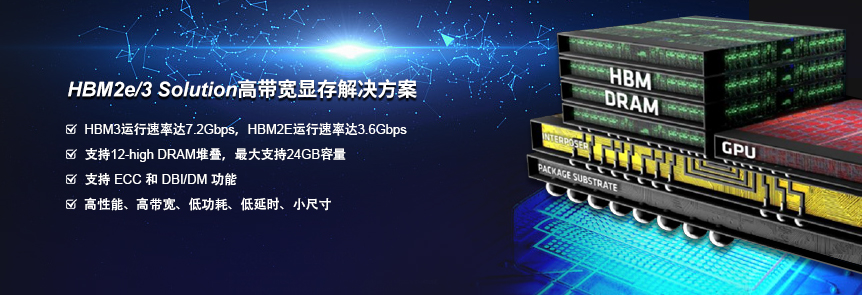
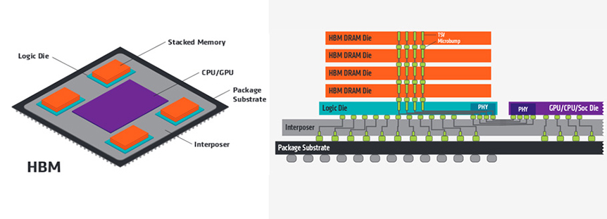
JESD235C 标準概述的第三代 HBM (HBM2e/3) 技術(shù)繼承了具有 2n/4n 預取架構、内部組織、1024 位輸入/輸出、1.2 VI/O 和(hé)内核電壓的物理 128 位 DDR 接口作為 以及原始技術(shù)中(zhōng)的所有關(guān)鍵部分。 與前代産品一樣,HBM2e/3 在每個(gè) KGSD 的基本邏輯芯片(2Hi、4Hi、8Hi、12Hi 堆棧)上支持兩個(gè)、四個(gè)、八個(gè)或十二個(gè) DRAM 設備。 HBM Gen 3 将堆棧内 DRAM 設備的容量擴展到 24GB,并将數據速率提高到每個(gè)引腳 7.2Gb/s。 此外,新技術(shù)帶來了帶寬最大化的重要改進。

INNO HBM2e/3 是 Innosilicon 廣泛的前沿内存PHY和(hé)控制器(qì)controller IP 産品組合的一部分,其它還包括 GDDR6/6X 和(hé) DDR5/LPDDR5。 Innosilicon 産品系列由具有豐富專業(yè)知識的經驗豐富的團隊開發,使客戶能夠獲得最佳設計結果,同時加快上市時間。

The third-generation HBM (HBM2e/3) technology, outlined by the JESD235C standard, inherits physical 128-bit DDR interface with 2n/4n prefetch architecture, internal organization, 1024-bit input/output, 1.2 V I/O and core voltages as well as all the crucial parts in the original technology. Just like the predecessor, HBM2e/3 supports two, four, eight or twelve DRAM devices on a base logic die (2Hi, 4Hi, 8Hi, 12Hi stacks) per KGSD. HBM Gen 3 expands the capacity of DRAM devices within a stack to 24GB and increases the data rate by up to 7.2Gb/s per pin. In addition, the new technology brings an important improvement to bandwidth maximization.

The INNO HBM2e/3 is part of Innosilicon’s broad leading-edge memory IP portfolio that includes GDDR6/6X and DDR5/LPDDR5. Developed by the experienced team with great expertise, the Innosilicon product family enables customers to achieve the best design results while accelerating time to market.

KEY FEATURES:

  • Data rate up to 7.2Gbps with HBM3, up to 3.6Gbps with HBM2e

  • Supports 12-high DRAM stack with capacity up to 24GB per stack

  • Up to 920GB/s of data bandwidth for each cube with HBM3

  • Up to 460GB/s of data bandwidth for each cube with HBM2e

  • ECC and DBI/DM supported

  • Programmable 18mA driver with calibration

  • Multiple receivers for power and speed trade off

  • Balanced clock tree to reduce skew among bits

  • Various clock gating and low power modes

  • Measures taken to reduce simultaneous switching power/noise, for both DBI on and off

  • Self heating and aging effect carefully evaluated, IR/EM fixed to the best possible

  • Supports micro-bump and TSV package

  • Interposer routing straightly across Controller and DRAM with unified routing length for all bits

  • Interoperability test supporting any third-party DFI 4.0-compliant memory controller

  • IEEE1500 port supported for separate direct access to the memory stack and PHY

INNOSILICON ADVANTAGES:

  • Substantially increases bandwidth available to computing devices

  • Fully pre-assemble design, drop-in hard macro to ease integration and speed time to market

  • Offers leading performance, power, and area per terabit

  • Extensive EDA tool support for various design automation flows

  • DFT functions to reduce test time and ensure high test coverage

  • Proven capabilities in PHY and silicon interposer design and integration

  • Optional PI/SI and thermal co-design service

  • Full support from IP delivery to production

BLOCK DIAGRAM:

EXAMPLE APPLICATIONS:

一鍵啟動(dòng),簡化您的下(xià)一個(gè)産品設計流程!


聯系
我們

定制
需求