Innosilicon PCIe 4.0 PHY和(hé)控制器(qì)controller IP旨在最大限度地提高高性能計算中(zhōng)複雜系統環境中(zhōng)的接口速度。 它是一種低功耗、面積優化、經過芯片驗證的 IP,采用面向系統的方法設計,可(kě)為我們的客戶最大限度地提高靈活性并簡化集成。 PCIe 4.0 PHY 支持 PCIe 4.0、3.0、2.0 和(hé) 1.0,并全面支持可(kě)制造性。
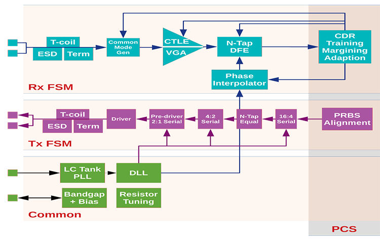
Innosilicon PCIe4.0 PHY 是一種高性能串行鍊路(lù)子(zǐ)系統。 我們的 PCIe 4.0 PHY 針對具有挑戰性的高插入損耗通(tōng)道的功率進行了優化,是網絡、存儲和(hé)數據中(zhōng)心系統的理想選擇。
The Innosilicon PCIe4.0 PHY is designed to maximize interface speed in the complex system environments found in high-performance computing. It is a low-power, area-optimized, silicon-proven IP designed with a system-oriented approach to maximize flexibility and ease integration for our customers. The PCIe4.0 PHY supports PCIe 4.0, 3.0, 2.0 and 1.0 and has full support for manufacturability.
The Innosilicon PCIe4.0 PHY is a high-performance serial link subsystem. Optimized for power in challenging, high-insertion-loss channels, our PCIe4.0 PHYs are ideal for networking, storage and data center systems.


 官方公衆号
官方公衆号 招聘公衆号
招聘公衆号